
SEMICON Japan 2025
- Event Date(s)
December 17-19, 2025
10:00 am - 5:00 pm JST
- Venue
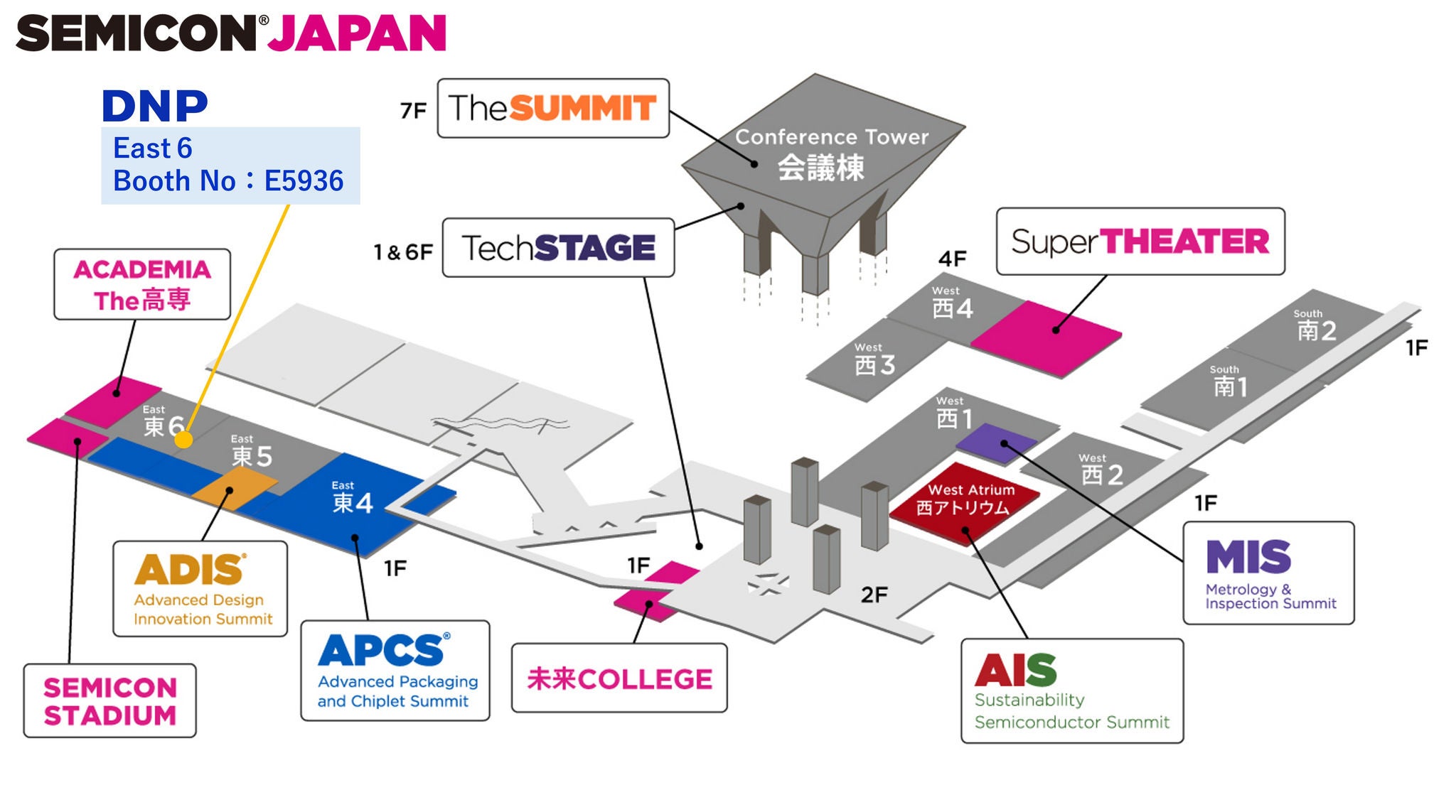
Tokyo Big Sight, Tokyo, Japan
(申込締切日や外部サイトに飛ぶなど注意事項を記載)
Registration has closed.
SEMICON Japan 2025

SEMICON Japan is the premier event that brings together the semiconductor manufacturing supply chain for the latest insights, trends, and innovations as the industry powers digital transformation. SEMICON Japan 2025 will highlight Smart applications powered by semiconductor technology such as automotive and Internet of Things (IoT).
Exhibited products
DNP is currently focusing on solving social issues and creating new values that meet people's expectations by synergizing our unique strengths P&I (printing and information) and extending collaboration with external partners.
Our products will be showcased at this exhibition: Extreme Ultra-Violet (EUV) lithography photomask, Nanoimprint Lithography (NIL) template, Co-packaged optics substrate, and other highly functional industrial materials.
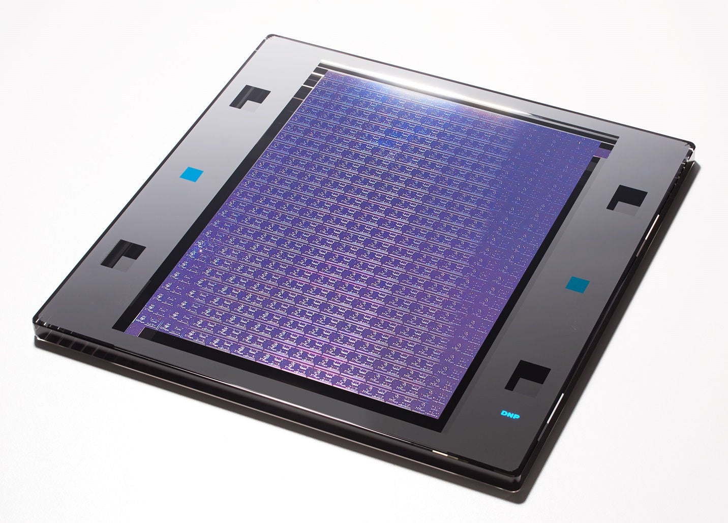
Extreme Ultraviolet Lithography(EUVL) Photomasks
A photomask with pellicle for EUV lithography, the most advanced semiconductor process.
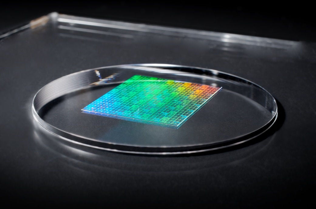
Nanoimprint Lithography (NIL) Template
A template for nanoimprint lithography. There are high expectations for this template as a new technology capable of supporting both shrinking chip structure and power consumption reduction in the semiconductor manufacturing process.
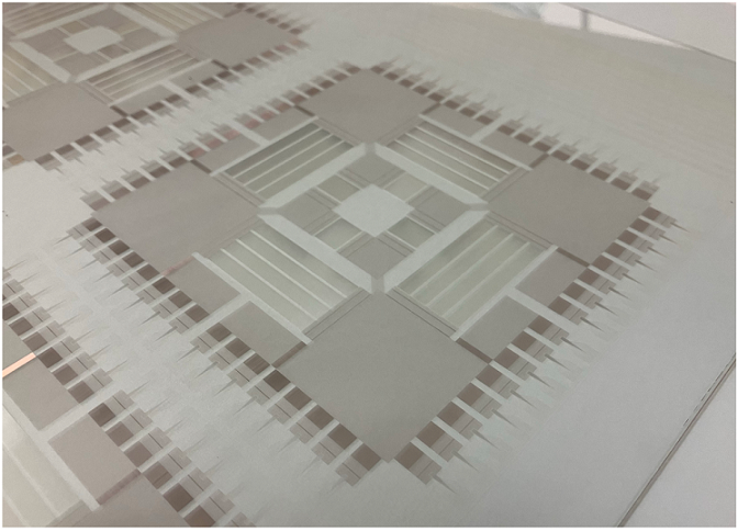
Co-packaged optics substrate
DNP will exhibit our glass wiring substrate with polymer optical waveguide, which is required in next-generation data centers where both power saving and high performance are needed.
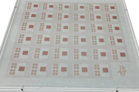
TGV Glass Core Substrate
We will exhibit high-aspect-ratio, narrow-pitch TGV glass core substrates and glass core substrates with wiring for advanced packaging.
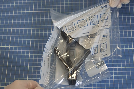
Ultra Clean Peelable Film(UCPF)
This clean packaging material is specifically designed for products such as semiconductors, electronic components, and precision parts, which require stringent particle and contamination control.
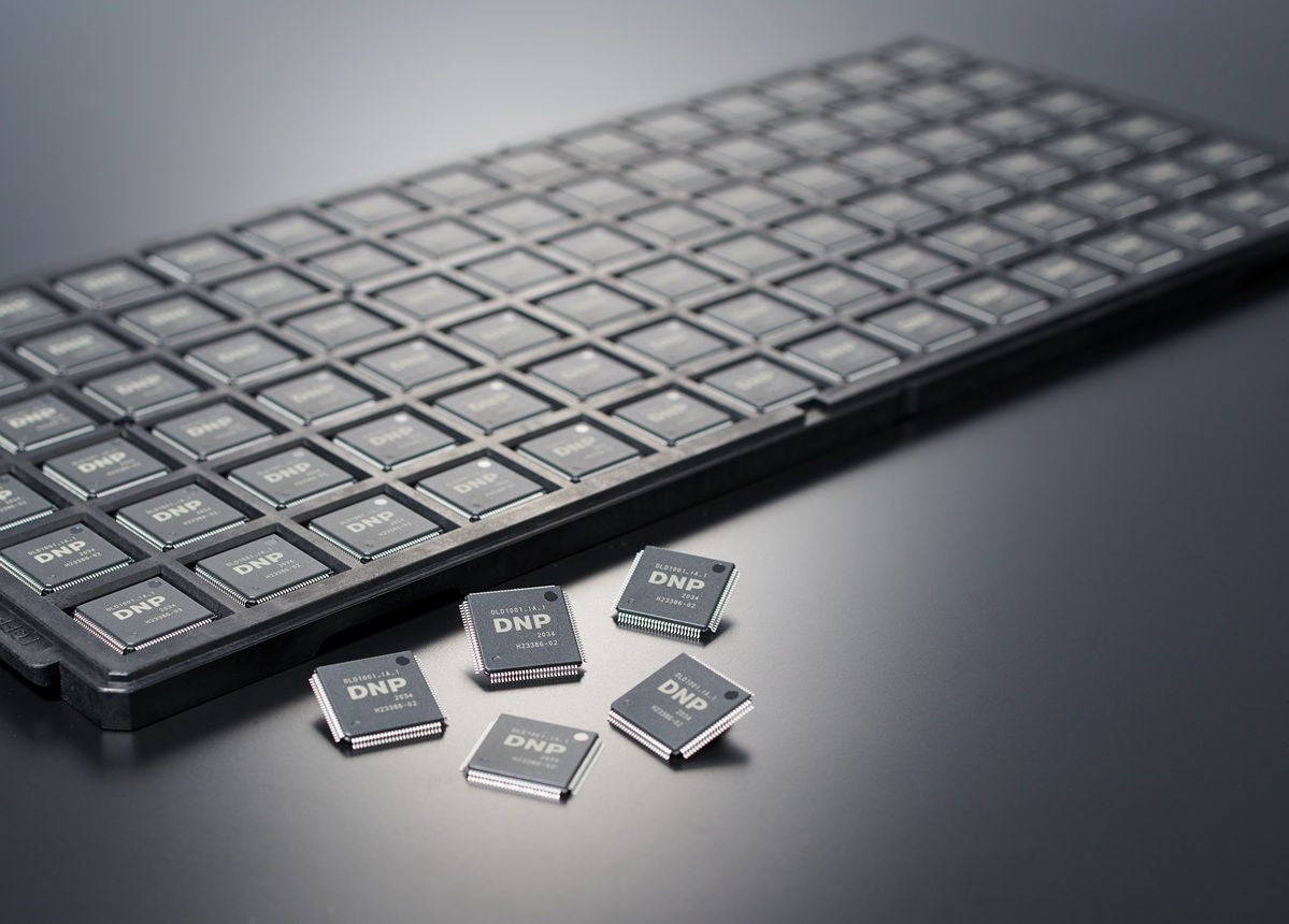
ASIC Development & Mass Production Solutions
We introduce DNP's ASIC design and development services. We will also exhibit sample chips.

3D Analysis of Semiconductor Devices
Introduction to a service that uses cutting-edge technology to visualize the complex structures of increasingly miniaturized and 3D-integrated semiconductors in three dimensions.
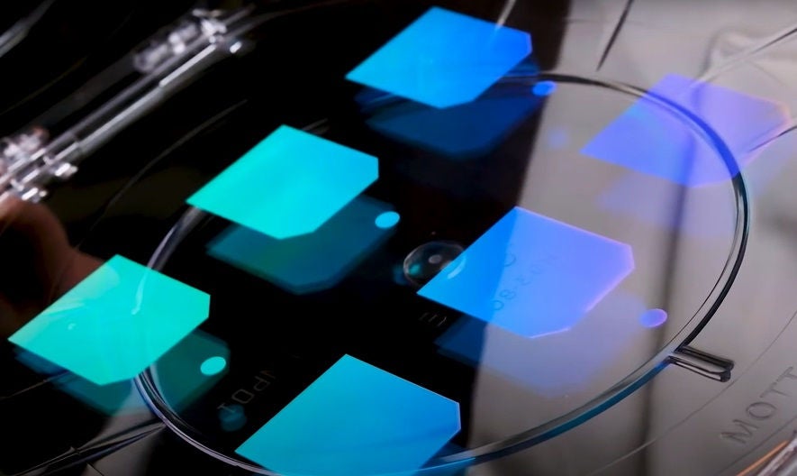
Quartz Master Mold Technology for Fabricating Optical Components
We provide one-stop services to meet customer needs for microfabrication, including nano-scale ultra-fine processing technology.
We will exhibit light guide plates for AR glasses and Qz master mold samples for micro lens arrays.
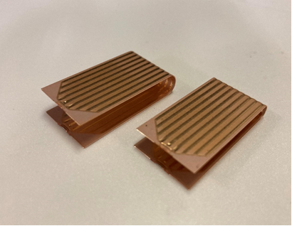
Application of metal microfabrication to semiconductor packages
We are developing products by combining new technologies with precision metal processing techniques. At this exhibition, we will showcase samples and technologies we have developed, including vapor chambers and metal-resin composite materials.