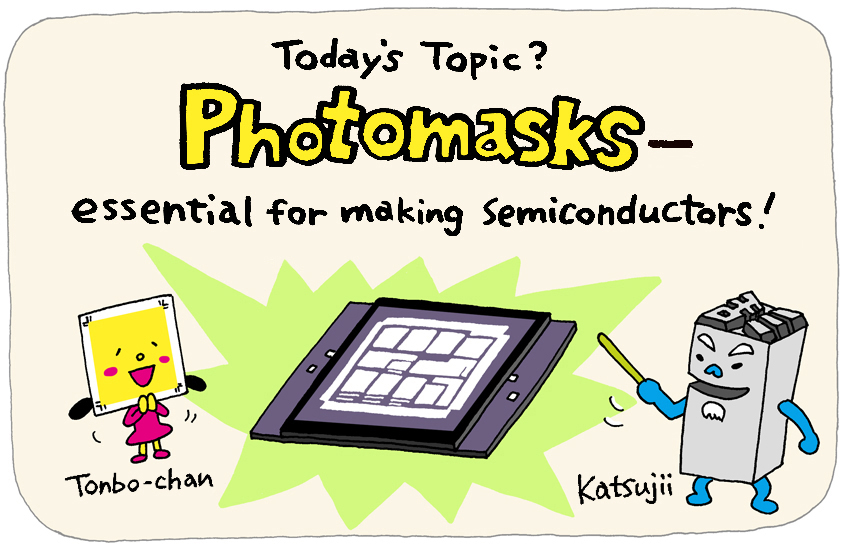
Semiconductors support our lives and are embedded in electrical applications, ranging from smartphones and vehicles to ATMs and home appliances. The most vital component in their manufacturing process is the photomask used to create fine circuit patterns. Since successfully prototyping a photomask in 1959, DNP has consistently taken on the challenge of developing diverse products and innovative technology. Now, it has become a major business pillar supporting the international semiconductor market. We will explore the secrets of DNP's photomasks.


Katsujii... Kinzoku Katsujii’s career as a movable type spans more than 100 years. With his many years of experience, he shares his extensive knowledge of the DNP Group, living up to his reputation as a walking dictionary.

Tonbo-chan... A character born from the "tonbo" (*) registration marks used to align printed materials. She has a meticulous personality, hates anything misaligned, and supports Katsujii with her careful attention to detail.
- [Printing term: registration] The precision of aligning each color plate in multicolor printing is called "registration." Registration is done using "tonbo," which are registration marks on the plate surface.
Photomasks determine semiconductor performance
Let us start by discussing semiconductors, which are used in manufacturing the photomasks that are today's focus.
Semiconductors are indispensable components in modern society, incorporated into everything from home appliances like rice cookers and microwave ovens to smartphones, computers, and automobiles. Originally a term describing the properties of materials, they are called semiconductors because they have properties between those of conductors, like metal, that easily conduct electricity, and insulators, like plastics, which resist the flow of electricity. This property allows them to switch an electrical current on and off, controlling devices.
Semiconductor performance depends on the precision of circuit patterns that control the flow of electricity. According to Moore's Law, proposed by Intel's founding members in 1965, the speed of circuit pattern refinement doubles every 18 months, with current minimum pattern sizes of about 12 nm (nanometers, one billionth of a meter). This is even smaller than the 100 nm influenza virus. Smartphones are one example of a product requiring high-performance semiconductors, and 2024 models are over 70,000 times more precise than the original model released in 2007.

One of the key components in manufacturing semiconductors is the photomask. It functions like photographic negative film and serves as the master template to transfer semiconductor chip circuit patterns onto a base material called a silicon wafer. In other words, no matter how precisely the circuit is designed, without a photomask that can transfer it accurately, semiconductors cannot be mass-produced.
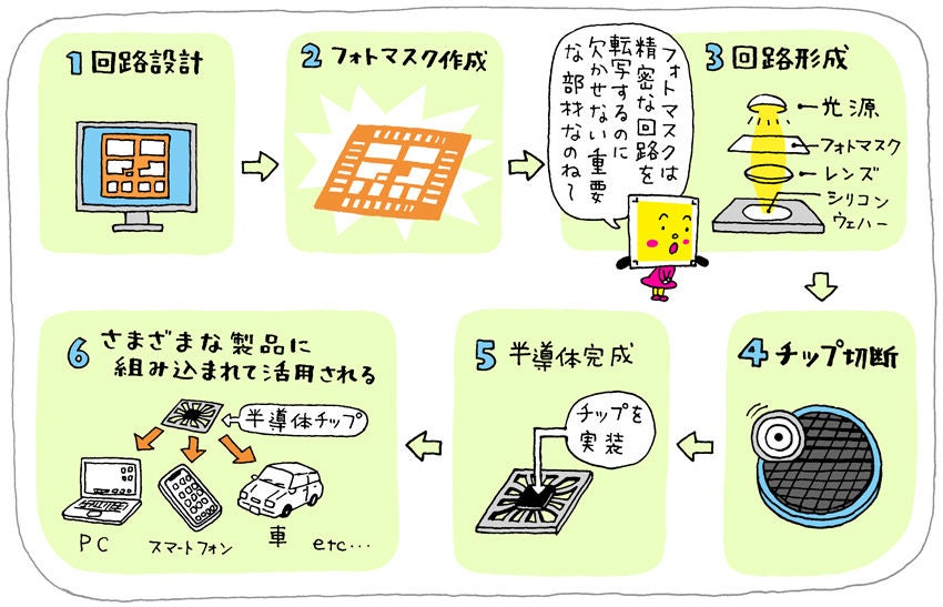 Semiconductor manufacturing process
DNP successfully developed photomasks for semiconductors in 1959 by combining microfabrication and optical design technologies that it had developed in printing processes. Since then, the company has continued to develop and supply semiconductor manufacturers with a range of high-definition photomask products.
The secret behind producing precision photomasks
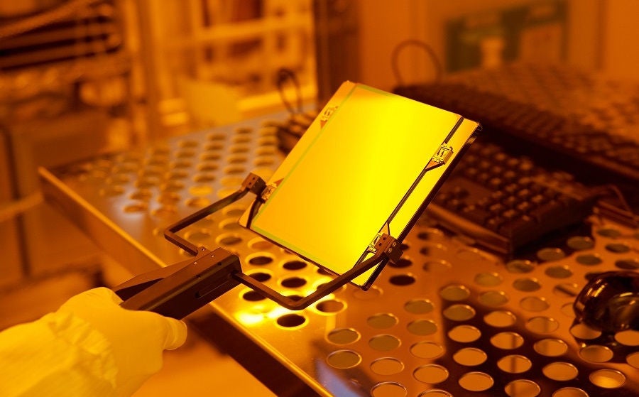
Now, let us look at how the photomask itself works. A photomask is a transparent, plate-like component with semiconductor chip circuit patterns drawn on glass, quartz, or other materials.
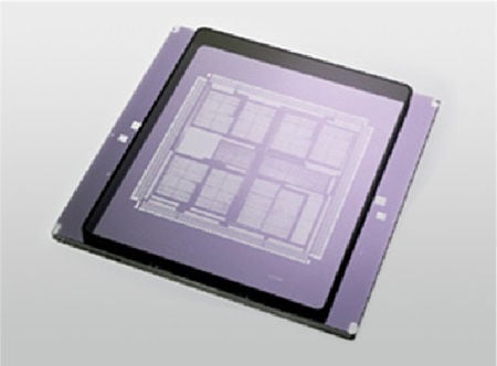 A typical photomask is about 150 sq mm. The circuit pattern is drawn in white on the flat, central part.
These photomask patterns, which are ultra-fine, are measured in nanometers (nm), or one hundred thousandth the width of a human hair. As such, their manufacturing requires advanced technology. DNP's photomasks are particularly precise, with few defects or foreign particles, and with dimensional uniformity of less than 1.5 nm and pattern misalignment of less than 2 nm. The sensitivity of the device, which uses light to detect defects, is 35 nm and inspects 100 sq mm in approximately 80 minutes.
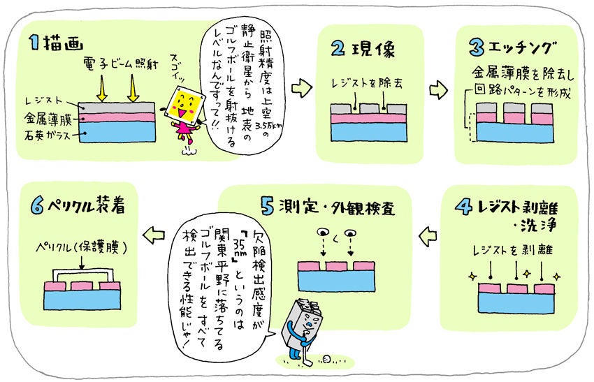 Photomask manufacturing process
In this way, DNP is able to manufacture high-quality photomasks through the technology, expertise, and manufacturing process innovations it has developed over many years.
DNP's goal for a future where cutting-edge technology is available to all
In recent years, the spread of generative AI, Virtual Reality/Augmented Reality, and autonomous driving, along with growing demand for large-scale data centers that support these technologies, has created demand for more advanced next-generation semiconductors. Next-generation semiconductors with faster processing speeds are expected to deliver environmentally friendly benefits such as longer battery life and reduced CO2 emissions from data centers. This has led to demand for photomasks that can transfer even finer circuits.
 Photomask for EUV lithography with protective film
The company has already completed development of the 3 nm generation process and has begun developing the 2 nm generation process.
Photomask for EUV lithography with protective film
The company has already completed development of the 3 nm generation process and has begun developing the 2 nm generation process.
However, while the adoption of EUV lithography is highly anticipated, it requires a large capital investment for new manufacturing equipment, making mass production difficult. Semiconductor manufacturers that cannot overcome the financial hurdles find it difficult to work in this cutting-edge field, and the widening technology gap between companies has become one of the challenges facing the semiconductor industry in recent years.
In response to these challenges, nanoimprint lithography (NIL) is anticipated to bridge the gap between conventional methods and EUV lithography. NIL is a semiconductor manufacturing method that creates ultra-fine circuit patterns by pressing a template onto a resin-coated substrate like a stamp. Its major advantages are "low power consumption" and "low cost," which can reduce power consumption during semiconductor manufacturing to about one-tenth that of conventional methods. DNP is currently working on mass NIL production. The development has attracted attention because it could enable more manufacturers to produce semiconductors incorporating this cutting-edge technology, leading to an overall boost in the semiconductor market.
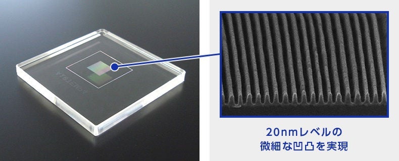 A nanoimprint lithography (NIL) template with ultra-fine irregularities of 20nm (left: appearance of NIL, right: magnified photo of NIL)
- DNP Features 半導体製造のカーボンニュートラルを加速する「ナノインプリントリソグラフィ」
https://www.global.dnp/ja/our-goals/media/2021/1206_20167700/
DNP will continue to develop in cutting-edge fields like EUV lithography, which is anticipated to grow further, while also working on mass production of NIL templates that will expand the range of low-cost, energy-saving product options. By meeting the demand for a wide range of photomasks and templates, we will contribute to the "democratization" of cutting-edge semiconductor manufacturing. This will enable many companies to make use of the technology, helping create a society where everyone can enjoy user-friendly services and devices. Thus, DNP will strive to be the catalyst of a better future.

Considering how important semiconductors are, the responsibility of developing photomasks is huge.

I hope they will keep working hard, knowing how much DNP can help the world.
- Please note that the information contained in this story was accurate as of the publication date.
更新日:2025年11月6日
First published: September 24, 2024 by DNP Features Editorial Department
