DNP Accelerates Development of Photomask Manufacturing Process for 2nm Generation EUV Lithography
Participate in NEDO R&D Project as Rapidus subcontractor
Mar 27, 2024
Tokyo, March 27, Dai Nippon Printing Co., Ltd. (DNP) has begun full-scale development of a photomask manufacturing for 2-nanometer (10-9 meter) generation logic semiconductors that support Extreme Ultra-Violet (EUV) lithography, the cutting-edge process for semiconductor manufacturing.
In this latest development, DNP will also act as a subcontractor and provide the newly developed technology to Tokyo-based Rapidus Corporation (Rapidus). Rapidus is participating in the Research and Development Project of the Enhanced Infrastructures for Post 5G Information and Communication Systems instigated by the New Energy and Industrial Technology Development Organization (NEDO).
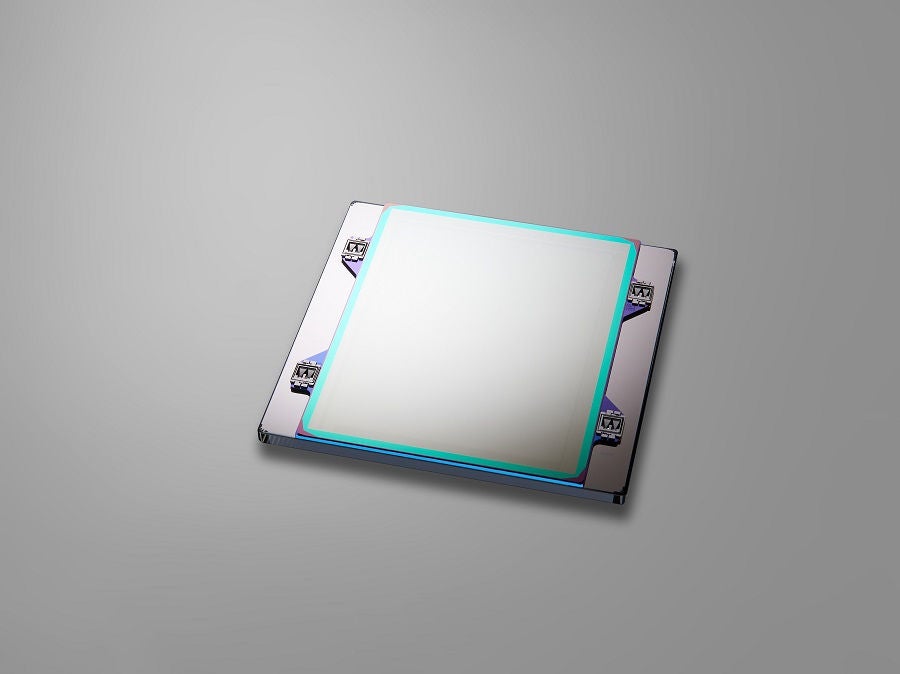
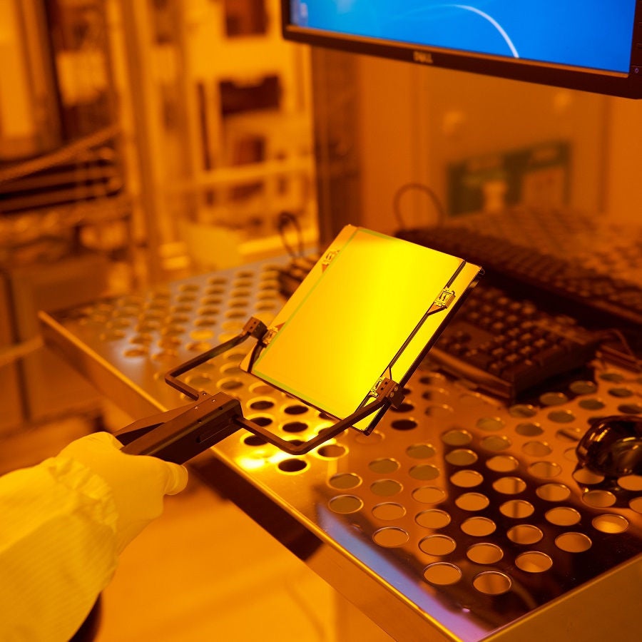 Image of EUV lithography with pellicle1, a protective film for the photomask
[Background]
In recent years, advances have been made in the production of cutting-edge logic semiconductors using EUV.
We have strengthened our ability to manufacture cutting-edge semiconductors with high productivity and quality. And in 2016, DNP was the world's first merchant photomask manufacturer to introduce the multi-beam mask writing tool (MBMW) 2.
In 2023, we completed the development of a photomask manufacturing process for 3-nm generation EUV lithography3, and commenced development of 2-nm generation technology. In response to the need for further miniaturization, we will begin full-scale development of a photomask manufacturing process for 2-nm generation EUV lithography, including the operation of second and third multi-electron beam mask lithography systems in FY 2024.
DNP plans to bring online its second and third MBMW mask lithography systems in FY 2024, accelerating the development of photomasks for 2-nm generation EUV lithography.
DNP will act as a subcontractor on Development of Advanced Semiconductor Manufacturing Technology (Commissioned) by Rapidus as part of the NEDO’s previously mentioned R&D project.
[Going Forward]
By FY 2025, DNP will complete the development of a manufacturing process for photomasks for 2-nm generation logic semiconductors that support EUV lithography. From FY 2026 onwards, we will push ahead with the establishment of production technology with a view to commencing mass production in FY 2027.
We have also begun development with an eye toward the 2-nm generation and beyond, and have signed an agreement with imec, a cutting-edge international research organization headquartered in Leuven, Belgium, to jointly develop next-generation EUV photomasks. DNP will continue to contribute to the growth of Japan's semiconductor industry by promoting development in collaboration with various partners within the framework of the international semiconductor industry.
1: A pellicle is a technical term for a thin skin, membrane, or film.
When transferring circuits for 2-nm generation semiconductors, if foreign matter adheres to photomasks for EUV lithography, there is a risk of lowering semiconductor manufacturing yields. DNP will promote the development of a photomask manufacturing processes for EUV that employ such pellicles.
2: For further information please visit; DNP Introduces Multi E-Beam Mask Writer to Strengthen Next-generation Semiconductor Photomask Production System by Significant Reduction of Writing Time https://www.global.dnp/news/detail/20167043_4126.html
3: For further information regarding 3-nm generation EUV lithography, please visit: DNP Develops Photomask Process for 3nm EUV Lithography https://www.global.dnp/news/detail/20170124_4126.html
- Company and product names listed in this release are the trademarks or registered trademarks of those companies.
- Product specifications and service details referred to in this news release are current as of the date of the announcement. They may be changed without notice.