DNP to Launch New TGV Glass core Substrate Pilot Line at Kuki Plant
Sample shipments to begin early 2026
Dec 16, 2025
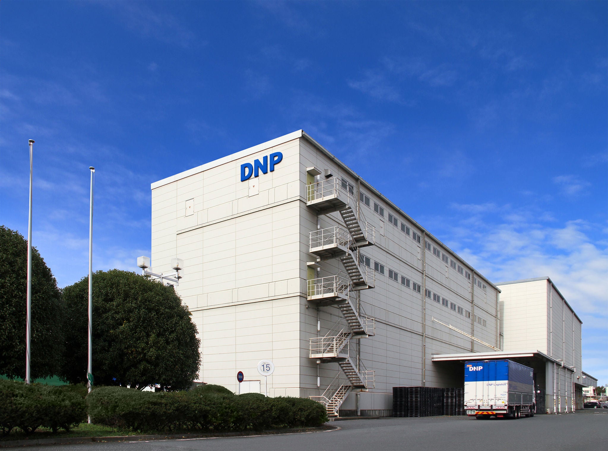
Tokyo, December xx, 2025, Dai Nippon Printing Co., Ltd. (DNP) will launch a new pilot production line for Through Glass Via (TGV) glass core substrates for next-generation semiconductor packaging at its Kuki Plant in Saitama Prefecture, Japan. The new line will commence phased operations from December 2025, enabling mass-production verification and the commencement of high-quality sample shipments in early 2026.
Background and Aims
The recent growth of generative AI is accelerating the adoption of chiplet architectures, in which multiple semiconductor chips with different functions are densely mounted on a single substrate to boost processing speed. Chiplets work to increase package sizes, but currently available organic-resin core substrates lack the required flatness, making it more difficult to form fine-pitch wiring. At the same time, insufficient rigidity leads to substrate warpage, making it difficult to mount semiconductor chips.
In order to resolve issues with next-generation semiconductor packaging platforms, DNP developed its TGV glass core substrate technology in 2023* as an alternative to conventional organic-core materials. The addition of the new pilot line for the manufacture of TGV glass core substrates, and samples delivery in early 2026 comes as numerous companies accelerate glass core substrates verification and conduct reliability assessments with a view to adoption.
The Kuki Plant has historically functioned as a publication-printing site. In building our new facility and system there, we look to optimize the plant's resources, including the workforce and space, and to promote the transformation of the DNP business-portfolio.
Key Features of DNP’s TGV Glass Core Substrate Samples
○TGV glass core substrates serve as the core material for Flip Chip-Ball Grid Array (FC-BGA), positioned between the motherboard and semiconductor chip. The formation of numerous fine through-hole electrodes enables electrical connection between the motherboard and semiconductor chip. By replacing existing organic resin with glass it becomes possible to arrange through-hole electrodes at a higher via density, enabling higher-performance semiconductor packages.
○Despite a relatively large size, at 510 × 515 mm, the substrate maintains the flatness and stiffness required for next-generation semiconductor packaging, and prevents warpage.
○Two types will be manufactured and offered: a "filled type," in which copper is filled into holes that penetrate the glass, and a "conformal type," in which a metal layer is adhered to the sidewall of the through hole.
○DNP aims to mass-produce substrates with high aspect ratios, featuring small via diameters relative to the glass thickness, where customer demand is strong and our fabrication expertise provides a competitive advantage.
Going Forward
DNP will begin providing TGV glass core substrate samples from the new pilot line in early 2026, and will build the structure required for full mass production in FY 2028 while closely monitoring client and market trends.
DNP will showcase the new product at SEMICON Japan 2025, to be held December 17–19 at Tokyo Big Sight, at the DNP booth situated at East Hall 6, E5936.
* For more information in Japanese about DNP’s TGV glass core substrate development, please visit: https://www.global.dnp/news/detail/20169052_4126.html
Company and product names mentioned in this release are the trademarks or registered trademarks of their respective owners.
Information contained in this release is current as of the date of announcement. It may be changed without notice.