Nano-Imprint Lithography (NIL)
Nano-Imprint Lithography is a technology that can fabricate the fine patterns required for high-performance semiconductors. It is possible to reduce the power consumption in the exposure process during semiconductor manufacturing to about 1/10 compared to the conventional technology.
Background
Semiconductor products with increasing performance due to the evolution of digital devices such as smartphones and tablet terminals, and the spread of 5th generation mobile communication systems (5G) and IoT. To achieve this, it is necessary to fabricate finer circuits, but since conventional technology uses enormous power in semiconductor manufacturing, new semiconductor manufacturing technology that consumes less power while achieving "pattern shrinkage" is required in recent years.
To solve these problems, DNP has developed "Nano-Imprint Lithography (NIL)", which is expected in the next-generation semiconductor manufacturing, based on the microfabrication technology experiences over many years.
What is Nano-Imprint Lithography?
Nano-Imprint Lithography is a technology to fabricate fine circuit patterns on the substrate in the order of nm (nanometers) using the ultra fine resin patterns which is formed by stamping the template (master) having surface morphologic patterns of circuit design onto the substrate coated with resin.
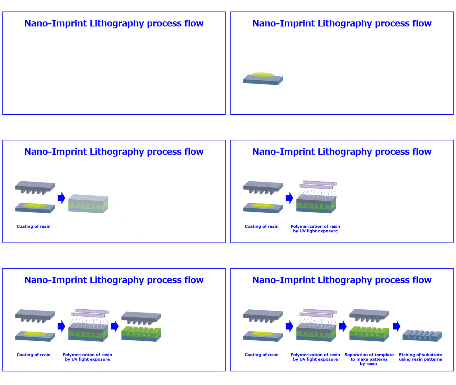
- Press the template (master) against the uncured UV curable resin coated on the substrate.
- Irradiate UV (ultraviolet) light to cure the resin.
- Release the template (master) to form resin patterns.
- The substrate with circuit patterns is fabricated by transfering the resin patterns into the substrate.
Power consumption reduced to 1/10 with Nano-Imprint Lithography
In recent years, semiconductors are required to have higher performance, and there is a concern of increasing power comsumption during manufacturing to achieve higher processing speed by pattern shrinkage and integration of the circuit. In addition, it is inevitable to reduce power consumption during manufacturing as a technical condition to support the semiconductor market, which is expected to expand due to the strengthening of digital infrastructure promoted by the Japanese government.
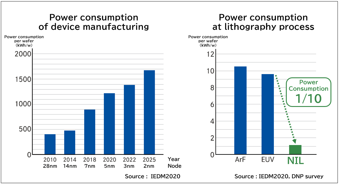
DNP has been developing a template (master) for Nano-Imprint Lithography since 2003, and we have succeeded to reduce the power consumption down to about 1/10 of conventional method by Nano-Imprint Lithography in the collaborative development between Canon Inc., Kioxia Corp. and DNP. We believe that this will greatly contribute to the realization of carbon neutrality for semiconductor manufacturers, along with the manufacturing cost reduction by this technology.
Click here for the development process
Future development: Creation of "3D template"
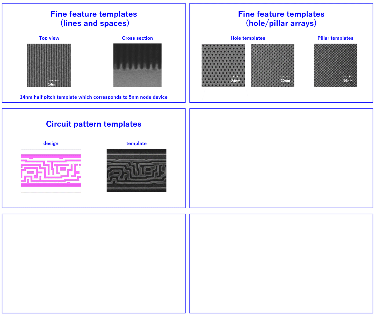
* All images in the video were taken with an electron microscope.
DNP is also developing a three-dimensional shape template which can realize three-dimensional pattern transfer on the substrate by utilizing the stamping characteristics of Nano-Imprint Lithography. By adopting this method, it is possible to form any of three-dimensional shapes, and it is expected to create new functions or devices that have never been realized before. We have already prepared templates with various three-dimensional shapes, and it is expected that they will be applied to 3D Nano-Imprint in the future.
Features of DNP Nano-Imprint Lithography
■ Low power consumption
Low power consumption at exposure process down to 1/10 compared to the conventional method
■ Environment-friendly
Environment-friendly with less use of chemicals
■ Low cost
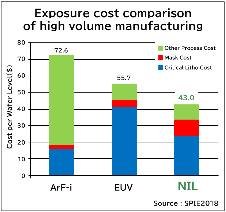
Low manufacturing cost woith less process steps and low equipment cost
■ Fine patterns
High degree of freedom in design because no light diffraction effect
DNP in Electronics
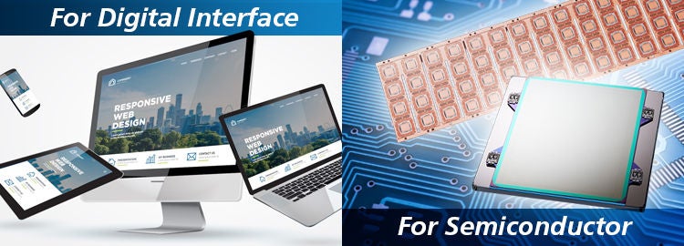
Other than listed above, DNP’s Electronics segment has a wide range of products for digital interface (display-related) and semiconductor.
You can check further our product line-up here and find anything to accommodate your needs.
