DNP to Exhibit at SEMICON Japan 2025
Will showcase EUV Lithography Photomasks, Next-Generation Glass-Core Substrates
Dec10,2025
Tokyo, December 10, Dai Nippon Printing Co., Ltd. (DNP) will exhibit at the internationally recognized semiconductor trade show, SEMICON Japan 2025 to be held from December 17 to 19, 2025 at Tokyo Big Sight.
DNP positions semiconductors as a focus business area. By leveraging proprietary core technologies including advanced microfabrication and precision coating, we develop essential products, such as semiconductor manufacturing photomask circuits, and next-generation packaging materials to deliver indispensable value across the entire semiconductor supply chain.
The DNP booth will be situated at East Hall 6, No. E5936, where visitors will find a wide range of products and services that support both front-end processes, including semiconductor design, as well as back-end processes, such as advanced packaging.
For more information about SEMICON Japan 2025 please visit : https://www.global.dnp/biz/eventseminar/event/20177608_4123.html
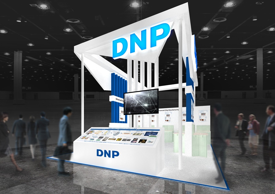
Image of DNP booth
Key DNP Exhibits
Front-End Semiconductor Manufacturing Related Products
Design and Development Support
Centered around DNP LSI Design Co., Ltd., we will present its contract services for Large Scale Integration (LSI) design, prototyping, and mass production, along with sample chips.
Photomasks for Semiconductor Manufacturing
DNP will showcase actual Extreme Ultra-Violet (EUV) lithography photomasks, equipped with protective film pellicles. The masks will feature Carbon Nanotube (CNT) pellicles that realize the high EUV transmittance required for cutting-edge semiconductor processes.
Nanoimprint Lithography (NIL) Templates
DNP will exhibit original templates used in nanoimprint lithography, a promising technology that is expected to enable further semiconductor miniaturization, reduced power consumption, and lower manufacturing costs. 3D sensors that support facial recognition and master templates for diffractive optical elements used in Augmented Reality (AR) glasses will also be on display.
Materials Analysis and Evaluation Services
DNP Scientific Analysis Center, Inc. will introduce its semiconductor chip and material analysis and evaluation services. The booth will also feature HOTSCOPE, a high-speed viewer software for displaying and analyzing photomask manufacturing data.
Functional Packaging Materials for Semiconductor Products
DNP will exhibit packaging materials for semiconductor products that leverage our proprietary lamination and coating technologies. Designed to meet the requirements of semiconductor manufacturing processes, these materials support higher efficiency and productivity across factory operations.
Back-End Semiconductor Manufacturing Related Products
Through Glass Via (TGV) Glass-Core Substrates for Next-Generation Packaging
DNP will exhibit TGV glass-core substrates, designed for high efficiency and large area applications and can replace conventional resin substrates. The high-density TGV structure facilitates the provision of higher-performance semiconductor packages than is currently possible.
Glass Panels for Co-packaged Optics Chiplet Integration
To help address the global challenge of rising data-center power consumption associated with the spread of AI, DNP will showcase opto-electronic co-packaged substrates with high-density optical waveguides designed to enable both high-speed, high-capacity data processing and energy efficiency.
*Product specifications and service details referred to in this new release are current as of the date of the announcement. They may be changed without notice.