DNP Develops Splicing Technology to Connect Multiple Nanoimprint Templates without Level Differences and with High Precision
Global first will facilitate mass production of scaled-up components
Dai Nippon Printing Co., Ltd. (DNP) has developed an innovative splicingtechnology that allows for the high precision connection of multiple nanoimprinttemplates, and which will facilitate the mass production of scaled-up components.
It is believed that this latest development marks yet another global firstfor the Company, which has also been achieved in answer to strong demand fromcompanies from a variety of industries.
Nanoimprinting is a micro-machining processing technology that takes materials,such as resin, formed on a substrate then seals them with a mold while stillsoft, before hardening to produce nanometer (10-9 meter) to micro-meter (10-6meter) level patterns in a stable manner.
DNP has offered DNP Nanoimprint Solutions since April 2015, asthe first one-stop response in the industry for companies looking for a totalpackage of services from template design, through prototype production to massproduction systems.
Looking ahead, the Company will take advantage of the newly developed technologyin the high precision micro-patterning of scaled-up templates.
[Background]
We are seeing the increased adoption of ultra-micro structures with the objectiveof providing new functionality and improving performance in display and opticalproduct components, as well as with energy- and life science-related components.There are also increased demands for large-area nano-level nanoimprints thatwill allow for an expansion in applicable products.
To date, ultra micro-processing with dozens of nanometer-scale patterns hasbeen limited to photomasks for semiconductors in sizes of approximately 15cm2,and in order to scale-up to bigger sizes it has been necessary to splice templatestogether. This, however, has produced the challenge of an uneven joint betweenthe spliced sections, and even where it has been possible to limit the differencein surface level to several dozen of nm, problems have arisen as the differencein level has had an adverse impact on lithography resist imprints, making itdifficult to employ this technology in production.
In order to overcome this challenge, DNP has forged ahead with the developmentof high precisions splicing technology that does not produce a difference inlevel when connecting separate templates, and by calling on an innovative technologyhas successfully done away with the difference in level. As a result, it isnow possible to produce ultra-micro structure scaled-up templates, and massproduce components, both of which have been in strong demand from numerous companiesin a variety of industries.
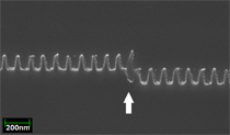
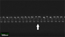
Cross section photograph of template.
At left, a template exhibiting a level difference betweenthe spliced templates.
At right, the spliced templates without a level differencebetween them, produced with DNP innovative technology
[High Precision Splicing Technology]
In this latest development, DNP has applied materials technology, processingtechnology and equipment technology developed using nano-level imprints, includingphotomasks and nanoimprint lithography (NIL) for semi-conductors , and the ultra-lowreflective film to develop a high precision splicing technology for templateswith dozens of nm scale ultra-fine indentations.
By using this technology that does away with the level difference of severaltens of nm between the spliced portions of the templates, it is now possibleto scale-up to large templates with micro-patterning equivalent to photomasksor NIL templates. This new technology is also expected to offer a solution tothe problems that have arisen from the adverse impact of the level differencegenerated with large templates employing lithography resist imprints.
[Looking Ahead]
The newly developed high precision splicing technology can be applied toa variety of components beginning with display components that demand ultra-finestructure patterning.
For example, by providing ultra-fine indentation patterning, it becomes possibleto offer functional film that allows for the control of light direction andits strength. And by applying this splicing technology to the manufacturingprocess of the functional film, positive effects, such as improved productivityare also foreseen compared to currently employed techniques.
Furthermore, by facilitating mass production of scaled-up components, thisnew technology will lead to the realization of energy saving large displays,and the conservation of the global environment. Significant positive effectsfrom the configuring of large ultra-fine structures are also possible, and basedon this newly developed technology DNP will push ahead with the adoption offacilities capable of accommodating scaled-up templates.
The Company will focus efforts on sales of the new product and DNP NanoimprintSolutions, aiming for sales of a total of 60 billion yen in the three fiscalyears from 2018 to 2020.
* Product prices, specification and service contents mentioned in this newsrelease are current as of the date of publication. They may be changed at anytime without notice.
- Select location
-
- Category
-