DNP Develops Photomask Process Targeting 5nm EUV Lithography
Uses MBMW to achieve high productivity and precision
Dai Nippon Printing Co., Ltd. (DNP) is pleased to announce the development of a photomask process capable of accommodating 5nm Extreme Ultra-Violet (EUV) lithography, a state-of-the-art semiconductor manufacturing process. The new process employs the multi-beam mask writing tool (MBMW) installed and used by DNP in 2016.
【Overview】
In current semiconductor chip production, circuit patterns are formed on silicon wafers using a photolithography technique. However, pattern resolution for chip production is limited by the argon fluoride (ArF) wavelength light source. In order to overcome this challenge, a next-generation lithography technique, EUV lithography with a 13.5nm wavelength light source, is applied and makes it possible to form circuit patterns with lengths of only several nm. Commercialization of EUV lithography for microprocessors based on a 5-7nm logic node process, and advanced memory devices, has begun at a small number of semiconductor chip makers, but is expected to spread to other semiconductor manufacturers engaged in cutting-edge processes.
In 2016, DNP became the world’s first merchant photomask manufacturer to adopt the MBMW(*1). In doing so, DNP answered the expectations of semiconductor chip makers with high quality and productivity, including the achievement of a significant shortening in writing time for next-generation photomasks.
In this latest development, by capitalizing on the advantages of MBMW, DNP has successfully developed a photomask process for high-precision EUV lithography capable of accommodating 5nm processes.
[MBMW Features]
- Utilizes approximately 260,000 electron beams allowing for a significant shortening in the writing time for complex patterns, including curvilinear patterns.
- Enables the use of low sensitivity resists that are essential to improve the patterning capability.
- The high-precision movement stability of the linear stage makes it possible to improve writing performance.
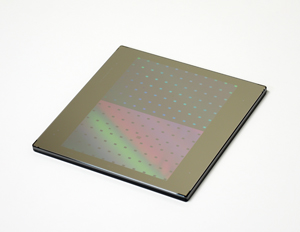
At left, high precision EUV photomask capable of accommodating 5nm processes
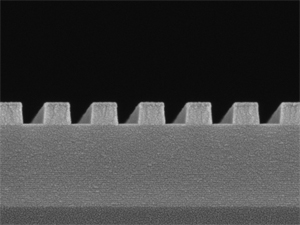
At right, enlarged cross sectional photo of the same
[Looking Ahead]
DNP will provide photomasks for EUV lithography to semiconductor chip makers, semiconductor development consortiums, equipment makers and material makers, and will support development relating to EUV lithography.
DNP targets sales of 6 billion yen per year in FY 2023.
Through joint development with partners, such as the world-leading research and innovation hub Interuniversity Microelectronics Centre (imec) headquartered in Leuven, Belgium, DNP will forge ahead with the development of advanced photomasks for next-generation Complementary Metal Oxide Semiconductor (CMOS) processing beyond 5nm.
DNP provides various solutions to support the advanced information society targeted by Society5.0 as an ultra-smart society. In particular, DNP will employ nanofabrication technology, based on DNP’s printing processes, to support high-performance semiconductors that are indispensable to the advanced information society. DNP will also strengthen the supply system for advanced photomasks for semiconductors that is expected to see further growth in demand.
*1 For further information please visit https://www.global.dnp/news/detail/20167043_4126.html
* Product prices, specifications and service contents mentioned in this news release are current as of the date of publication. They may be changed at any time without notice.
- Select location
-
- Category
-