DNP Introduces Multi E-Beam Mask Writer to Strengthen Next-generation Semiconductor Photomask Production System by Significant Reduction of Writing Time
Introducing a multi-electron beam mask writer to dramatically reduce writing time
December 13, 2016
Dai Nippon Printing Co., Ltd. (DNP) will strengthen its next-generation semiconductorphotomask production system by introducing a multi e-beam mask writer to achievesignificant reductions in writing time.
[Challenges]
Currently available semiconductors are experiencing a shift to miniaturization,including configuration of 3D stacked some dozen nanometer circuits on siliconwafers. At present semiconductor manufacturing employs photolithography technology,but depending on the characteristics of light wavelengths, resolution is limitedin some cases, and recourse is had to such technologies as multi-exposure thatconfigures multiple photomasks onto a single layer, and optical proximity correctionthat configures photomasks with complicated patterns corrected for light attributes. With multiple exposure technology, however, it is necessary to increase thephotomask count, while optical correction technology entails a lengthy patterningperiod for each photomask. Hence, manufacturing next-generation photomask forthe 10nm or less process requires several days for the writing process alone,and as it has been anticipated that the required amount of time may become evenlonger in the shift to further miniaturization, there have been calls for amanufacturing methodology capable of reducing writing time.
In response, as a merchant photomask maker, DNP will strengthen its semiconductorphotomask production system by introducing the world’s first* multi e-beammask writer, to achieve significant reductions in photomask writing time, andto facilitate high productivity.
- as of November 2016
[Multi E-Beam Mask Writer]
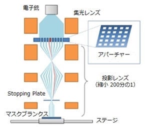
DNP has cooperated with semiconductor and lithography device manufacturers for aperiod of approximately five years in developing the multi e-beam mask writer.By utilizing a special aperture that controls light volume, with the new deviceit is possible to fire approximately 260,000 e-beams from a single electrongun. With existing techniques, next-generation photomask writing has requiredmore than 18 hours, and as much as several days depending on the minimum linewidth of the semiconductor circuit pattern. But, by achieving high e-beam precision,for photomask used in the 7nm process of each semiconductor manufacturer, itis now possible to reduce writing time to approximately 10 hours. Further timereductions will become feasible with next-next generation semiconductor photomasksas they increasingly shift to miniaturization.
Looking Ahead
In addition to strengthening the next-generation semiconductor photomasksupply system, DNP will also accelerate joint development with semiconductormanufacturers, at the same time as supporting production systems at each manufactureron a global basis, and endeavoring to achieve the standardization of next-generationsemiconductor photomask processes.The Company will also apply the multi e-beam mask writer in the manufactureof nanoimprint lithography templates used in 3D stacked NAND flash memoriesthat are expected to see significantly increased demand. DNP will further strengthen the miniaturization-driven next-generation semiconductorphotomask supply system, aiming for uses with the IoT-driven big data management,and artificial intelligence.
The Company aims for annual sales of 6.0 billion yen in FY 2019 as a resultof the strengthening of photomask manufacturing systems based on the multi e-beammask writer.
- Product prices, specification and service contents mentioned in this news release are current as of the date of publication. They may be changed at any time without notice.