DNP Develops TGV Glass Core Substrate for Semiconductor Packages
Contributing to higher performance semiconductors
Mar 20, 2023
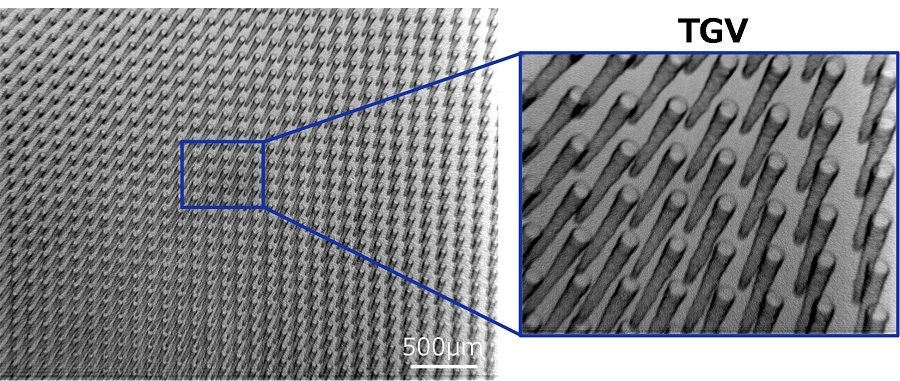
Tokyo, March 20, Dai Nippon Printing Co., Ltd. (DNP) has developed a Glass Core Substrate (GCS) targeting next-generation semiconductor packages. The new product replaces conventional resin substrates (ex. FC-BGA: Flip Chip-Ball Grid Array) with a glass substrate. Through the use of high-density Through Glass Via (TGV), it is now possible to provide a higher performance semiconductor package than that based on currently available technology. In addition, by adapting our panel manufacturing process, the new product can also support demands for high efficiency and large-scale substrate.
 X-ray image of TGV in the glass core substrate
Background
As Data distribution volume has increased dramatically in line with the advance of digital transformation (DX), there are demands for improved performance and increased reliability of the semiconductor devices that support social infrastructure. For this reason, the focus is on next-generation semiconductor packages with improved processing speed, driven by the high density mounting of multiple semiconductor chips with various functions on a single substrate. However, electrode-configuring technology, such as the chip/package interconnect substrate, or Interposer*1 (ex. GIP: Glass Interposer), pose challenges, such as difficulty in achieving fine pitching of extremely narrow wiring, along with the large-scale substrate of semiconductor packages.
In this latest development, DNP focused on glass as a substrate for semiconductor packages, and has developed a GCS that configures fine TGV with a high aspect ratio compatible with the fine pitch. Aspect ratio refers to the ratio of glass thickness to the via diameter, where the higher the ratio the more difficult it is to process.
- 1 DNPのインターポーザ → https://www.dnp.co.jp/news/detail/10161685_1587.html
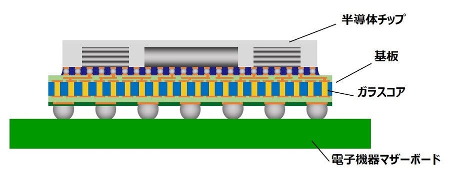
 Where glass core substrates are used
Product Features
Achieves fine pitch and high reliability
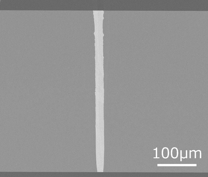
The newly developed GCS includes a TGV necessary for electrically connecting the fine metal wiring configured on the front and back of the glass. It is a Conformal Type glass substrate in which a metal layer is adhered to the side walls of the Via. Our new proprietary manufacturing method enhances the adhesion between glass and metal, which was difficult to achieve with conventional technology, to realize fine pitch and high reliability.
 Cross section of Conformal Type glass substrate
Achieves high aspect ratio and large-scale
TGV with a high aspect ratio is necessary to conduct high volume signal transmission on a limited scale. The newly developed glass substrate has an aspect ratio of 9+, and maintains sufficient adhesive qualities to configure fine wiring. As there are few restrictions regarding the thickness of the glass substrate used, it is possible to boost the degree of freedom when designing warpage, rigidity, and flatness. At the same time, it is also possible to accommodate package scalability by employing our panel manufacturing process.
Looking Ahead
In addition to the existing Filling Type glass substrate that fills the glass via with copper, DNP is also promoting the scalability of the newly developed Conformal Type glass substrate to a panel size of 510 x 515mm. We aim for sales of 5.0 billion yen in FY 2027.
DNP has leveraged its core technology of Microfabrication Technology that applies and develops printing processes to offer semiconductor photomasks and Micro Electro-Mechanical System (MEMS) foundry services. In this latest development, we have applied technologies developed through such businesses, including our proprietary panel manufacturing process technology along with the technology designed for handling large-scale glass, to develop a glass substrate. Going forward, we will leverage our strengths in printing and information (P&I), such as combining electronic components with those in Information Technology, including information security, to provide solutions that will support a pleasant information society.
 Filled type glass cross section image
*All company and product names mentioned herein are the trademarks or registered trademarks of their respective owners.
* The information contained in this release is current as of the date of announcement and is subject to change without notice.
